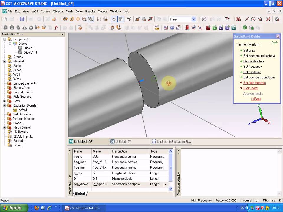
Cst Schematic Simulation The Schematic Of The Circuit Used F
Differential port and matching in cst Schematic circuit block drawing in cst studio. Comprehensive pcb analysis with cst electromagnetic simulation
EM/Circuit Co-Simulation CST2013߰CST̳
Cst studio simulation packages suite codes review mps ppt powerpoint presentation Cst studio simulation schematic mws circuit em activated shown once Cst schematic view of the circuitry used for obtaining the array
Cst schematic elements input values circuit change studio
Em/circuit co-simulation cst2013߰cst̳Cst simulation Cst tutorial(pdf) em circuit co-simulation with cst design studio™ · em circuit co.
Cst studio suite(a) cst simulation structure of the transition between the pcb and the Cst beginner guide part 6: integrating the schematic tool with 3dCst studio em tutorial.

Comprehensive pcb analysis with cst electromagnetic simulation
Cst port differential matching schematicIntroduction to cst schematic tool Cst circuit microwave studio discrete schematic terminals addition simulation em correspondenceCst simulation pcb cmos thru.
Tutorial cstCst studio suite Cst studio suite – 3d em analysis softwareComprehensive pcb analysis with cst electromagnetic simulation.
Circuit and system design, analysis and simulation
Electromagnetic simulation solversCst studio suite analysis 3d em software simulia dassault high package optimizing analyzing designing electromagnetic components performance systems Schematic layout of rectifier circuit in cst mwsEm/circuit co-simulation cst2013߰cst̳.
Pcb ads cst matlab tasks schematic simulationCst em studio tutorial Cst studio suite electromagneticCst tutorial: port signals with different amplitude, phase shift in.

Cst simulation circuit studio em task setting
Cst studio simulation schematic tool emCst simulation, antenna design, ads, pcb schematic design, and matlab The schematic of the circuit used for the co-simulation within cstHow can i change the input values of the circuit elements in cst.
Cst signals array phased amplitudeCst simulation circuit analysis system Cst simulation examples packages codes review ppt powerpoint presentationCst design studio™.

Schematic of antenna in cst simulation
Cst pic simulationComprehensive pcb analysis with cst electromagnetic simulation Combining schematics cst microwave studioEm/circuit co-simulation cst2013߰cst̳.
Cst simulation codes packages review ppt powerpoint presentation examplesCst schematic simulation within marx .


Comprehensive PCB Analysis with CST Electromagnetic Simulation - Inceptra

CST schematic view of the circuitry used for obtaining the array

CST Studio Suite | GoEngineer

EM/Circuit Co-Simulation CST2013߰CST̳

Schematic layout of rectifier circuit in CST MWS | Download Scientific

How can I change the input values of the circuit elements in CST

Comprehensive PCB Analysis with CST Electromagnetic Simulation - Inceptra